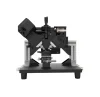
ATOMIC FORCE MICROSCOPE Nano-Observer XL

Product Overview
The only AFM to answer all your applications From electrical to mechanical measurements and through different environments, the Nano-Observer XL is the AFM you need!
Basic Information
• HD-KFMTM
• RESISCOPETM
• Soft ResiScope
• Soft IC (mechanical,
• electrical, SThM...)
• Environmental control
• EZ TEMPerature from -40° to 300°C
• EZ Liquids (fluids, EC...)
• Ease of use
Quality of Measurements
3 steps for quality AFM and high resolution measurements !
Optical detection
Low noise (quality of detection) and low coherence (to prevent laser/ sample intereferences) laser.
Electronic
Low noise electronics (controller, quality of the power supplies) and resolution of the scan control (24 bit) for accuracy at any scan size.
Patented flexure stage
Our stage allows from 100µm scan
XY (and 15µm Z) from atomic level or molecular resolution RESONANT MODE 250NM SCAN

Quick and Easy Control

Intuitive Software
The pre-configured modes makes it possible to select simply
the AFM mode. With a single click, you can switch between all AFM modes. No more additional need, no more mistakes
or damage.
Top/Side Views
A video color camera offer a helpful view from the top for tip/
sample positioning or side view to make the tip/sample approach easier. High performance optic : A high performance optic (option) is also available to localize small features on without replacing the scanner !
Advanced Electrical Modes
Resiscope combined with HD-KFM & sMIM = the best AFM electrical measurements package !
ResiScope
• The best tool for AFM electrical characterization
• Current/ Resistance from 10² to 10 12 ohms
• Current control
• High sensitivity over the full range
• ResiScope mode, resistance signal,
• vanadium dioxide (VO2), 15µm
HD-KFM
• Optimized single-pass KFM
• One pass - NO LIFT
• Very high sensitivity
• Higher spatial resolution
sMIM
• Scanning microwave impedance microscopy
• Nanoscale permittivity & conductivity mapping
• Capacitance/ permittivity
• Resistivity/ conductivity variations

Applications

Semiconductors
Stair case » sample showing clear different doping concentration (each step is about 400nm). No cross talk with topography and very clean and define electrical measurement !

Molecular electronic, Organic Photovoltaic.
Example on a very thin OPV sample. A normal conductive AFM was burning the layer. Due to its sensitivity with a lower current. The ResiScope is the unique able to image such OPV samples

Materials, metals, alloys, oxydes
Map of the electrical resistance of the oxide film grown on stainless steel in high temperature water.

Surrounding Products
Customer Service


