Service

Micro-Nano Testing Services
Field Emission Scanning Electron Microscopy (FESEM)
Introduction: High magnification of 800,000 times, can be separated from the mobile phone and separate the signal of simple secondary electrons, mixed secondary electrons and backscattered electrons, when the acceleration voltage is 15kV, the high resolution can reach 1nm (depending on the sample), at the low acceleration voltage of 1kV, the deceleration function is not applicable, it can reach 2.0N.
Atomic Force Microscopy (AFM)
Introduction: Automated AFM and Scanning Tunneling Microscopy techniques can be used to measure the surface properties of semiconductor silicon wafers, etching masks, magnetic media, CD/DVD, biomaterials, optical materials, and other samples up to 200 mm in diameter.
Nano Indenter G200
Samples can be accepted: semiconductor devices, thin films, hard coatings, DLC films, composite materials, optical fibers, polymer materials, metal materials, ceramic materials, lead-free solders, biomaterials, biological and biomimetic tissues
Introduction: Main functions: Instrumented indentation and indentation at the nano/microscopic scale, mainly used to test the elastic modulus and indentation hardness, film critical adhesion and friction coefficient of small or thin film samples, etc. It has functions such as continuous stiffness test mode, in-situ indentation topography scanning, stiffness scanning and fast press-in testing. The main features

Equipment Training Services
D-500 Step Meter
Samples can be accepted: films, fibers, metals, etc Introduction: On-site installation, calibration, training, training content: basic use, calibration (linearity calibration, height calibration), stage leveling.
P-7 Step Meter
Samples can be accepted: films, fibers, metals, etc Introduction: On-site installation, calibration, training, training content: basic use, calibration (linearity calibration, height calibration), stage leveling.
Profilm 3D Optical Profiler
Samples can be accepted: glass, solar cells, semiconductors Introduction: Installation, training (training content, basic use, splicing), height calibration (other calibration needs to be confirmed by the manufacturer).
MTA03 Series
MVI-pifm
Samples can be accepted: optical materials and other samples Introduction: Installation, Training, Calibration, Adjustment of the Correction Optical Path..

Micro-Nano Processing Services
3D printing processing
Samples can be accepted: rigid resins, biocompatible resins, high-temperature resistant resins, flexible resins
Introduction: Provide global customers with scientific research and processing services such as printing mechanical metamaterials, three-dimensional complex bionic structures, biomedical devices, micromechanical structures, microfluidic samples, as well as industrial processing services such as connectors, endoscopes, and connectors.
Template customization
Samples can be accepted: templates
Introduction: The miniFactory Ultra 3D printer enables superpolymers and industrial-grade 3D printed parts to achieve ideal results. The industrial-grade high-temperature 3D printer solves the technical problem of how to print polymers well in a stable high-temperature
SiN Windows

Synchrotron Radiation Facility Testing Service
Beamline Test Service Introduction
The Soft X-ray scattering beamline of Shanghai Synchrotron Radiation Facility (SSRF) belongs to the soft branch of the energy materials research beamine (E-line) (BL20U2). It is one of the beamlines given birth by SSRF Beamlines Project (SSRF - Phase ll). It has passed CAS-process testing in October 2022 and is currently open to users. This branch beamine belongs to the E-line complex. It can operate completely independently as a soft X-ray beamline. It adopts an elliptical polarization oscillator (EPU60) as the light source and relies on a grating monochromator to deliver photons in the energy range of 130-150000eV to the experimental stations featured with soft X-ray scattering methods. These includes both inelastic methods such as Resonant Xray Emission (RXES) or Resonant Inelastic X-ray
Scattering (RIXS), and elastic methods such as Resonant Elastic X-ray Scattering (REXS) or Resonant Soft X-ray Scattering (RSOXS). These can be used to study electronic structures, e.g. fluorescence emission, charge transfer, d-d excitation etc or spatial structures, e.g. long-range orbital/spin/charge order, domain size/distribution for soft condensed matter (C.N,O) and inorganic materials including transition metals and rare earth, etc.

Fields Of Application

Energy Materials

Catalysts

Nano-Materials

Smart Materials

Soft Materials


Engineering of the catalytic site d-band structure based on RIXS:
This section is discussing how a technique called Resonant Inelastic X-ray Scattering (RIXS) was used to study the electronic structure of a material. Specifically, they looked at the d-band structure of nickel atoms in different environments: Ni@C, I-Ni@C, and I-Ni. The d-band is a region of energy levels associated with electrons in the d orbitals of the nickel atom. By understanding the d-band str
The key findings were:
• The energy required for electrons to move from the valence band (filled energy levels) to the unoccupied states (empty energy levels) increased in the order Ni@C, I-Ni@C, and I-Ni.
• The d-band center of these materials decreased in the same order.
• The moderate d-band energy level of I-Ni@C at the nickel site helped to balance the adsorption and desorption capacity of key intermediates, which is important for catalytic reactions.
• The material I-Ni@C showed excellent performance as a catalyst for the hydrogen evolution reaction (HER) in alkaline conditions.

Revealing the periodic structure of the cholesteryl phase of liquid crystal polymer materials:
This section describes how RIXS was used to study the structure of a liquid crystal polymer material. Liquid crystals have properties of both liquids and crystals. The cholesteryl phase is a specific type of liquid crystal structure.
The researchers used RIXS to investigate the near-carbon absorption edge of the polymer-stabilized cholesteryl phase under different polarization conditions. They found a diffraction peak corresponding to a one-dimensional periodic structure of the cholesteryl phase. This periodic structure has a half-pitch of 2132.6 nanometers.
In simpler terms:
Section 2 is about using a special technique to understand how electrons behave in a material that can be used as a catalyst. Section 3 is about using the same technique to study the arrangement of molecules in a type of liquid crystal. Both sections highlight the power of RIXS in understanding the properties of materials at the atomic level.
Would you like me to explain any specific terms or concepts in more detail?
For example, I could go into more depth about what the d-band is, how RIXS works, or what the hydrogen evolution reaction is.
Best Seller Service
P-7 step gauge
Brand: KLA
Samples can be accepted: films, fibers, metals, etc
Introduction: On-site installation, calibration, training, training content: basic use, calibration (linearity calibration, height calibration), stage leveling.
Features
• Step height: Nanometers to 1000µm
• Low force with constant force control: 0.03 to 50mg
• Scan full diameter of the sample without stitching
• Video: 5MP high-resolution color camera
• Arc correction: Removes error due to arc motion of the stylus
• Software: Easy-to-use software interface
• Production capability: Fully automated with sequencing, pattern recognition and SECS/GEM
Applications
• Step height: 2D and 3D step height
• Texture: 2D and 3D roughness and waviness
• Form: 2D and 3D bow and shape
• Stress: 2D and 3D thin film stress
• Defect review: 2D and 3D defect surface topography


Fields of Application
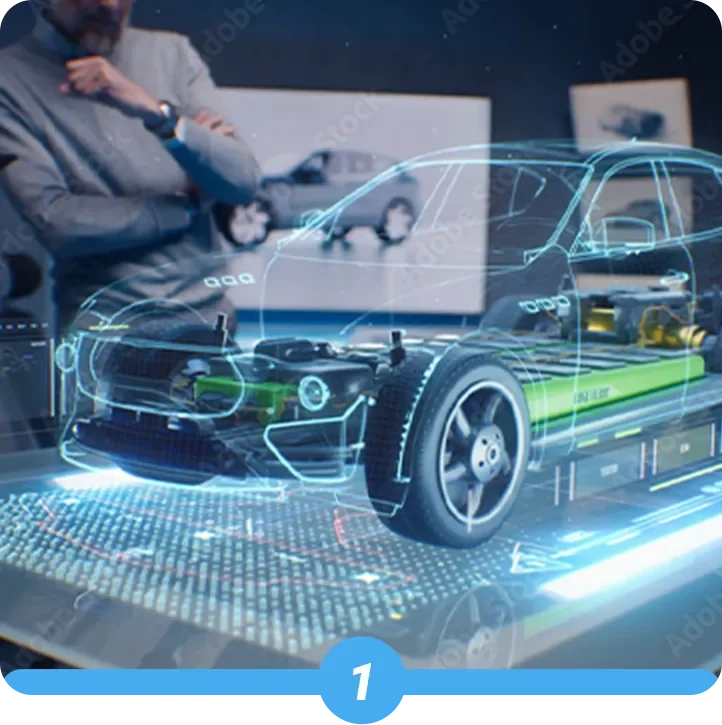
Automobile
Enhancing vehicle performance and safety through advanced material assessment.
Nanoscience
Enabling researchers to examine surfaces at the nanoscale, contributing to innovations in materials and devices.
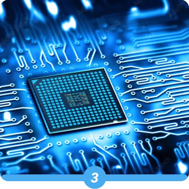
Semiconductor
Providing the precision required for semiconductor manufacturing, from wafer inspection to micro-level surface analysis.

General Consumables (Accessories)

AFM Accessories

SEM Consumables

TEM Consumables

SERS Chip Substrate

GGB Series


Customer Service


