
Wafer Warpage Stress Gauge
Wishlist
Product Description
Product Overview
It has the function of detecting three-dimensional warpage (flatness) and thin film stress, and is suitable for semiconductor wafer production, semiconductor process development, glass and ceramic wafer production
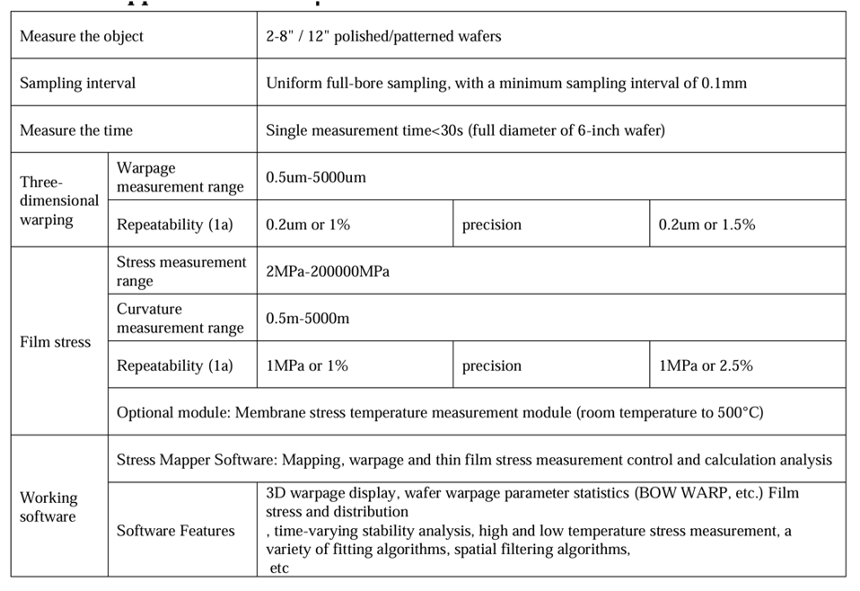
Basic Information
Application Direction
2 - 8 inch/12 inch polished wafers (silicon, gallium arsenide, silicon carbide, etc.), patterned wafers, bonded wafers, packaged wafers, etc.; Liquid crystal substrate glass; Surfaces treated by various film processes
Technical characteristics
Advantage
- Uniform sampling and measurement of all diameters, with a sampling interval of at least 0.1mm
- It has both warpage measurement and stress measurement functions
- Visualize the shape change caused by the thin film, and calculate the curvature and stress at any angle
- Powerful add-on module: Membrane stress temperature measurement module (RT to 500°C)
- Abundant software analysis functions, including: 3D warpage diagram, wafer warpage parameter statistics (BOW, WARP, etc.), ROI analysis, thin film stress and distribution, stress over time, thin film stress temperature measurement, curvature calculation, polynomial fitting, spatial filtering and other post-processing algorithms.
Fields of application
- Production and quality inspection of semiconductor and glass wafers
- Research and development of semiconductor thin film process
- Process control and failure analysis of semiconductor processes and packaging downgauging processes


Compare product
0/4
Remove all
Powered By
 MakeWebEasy